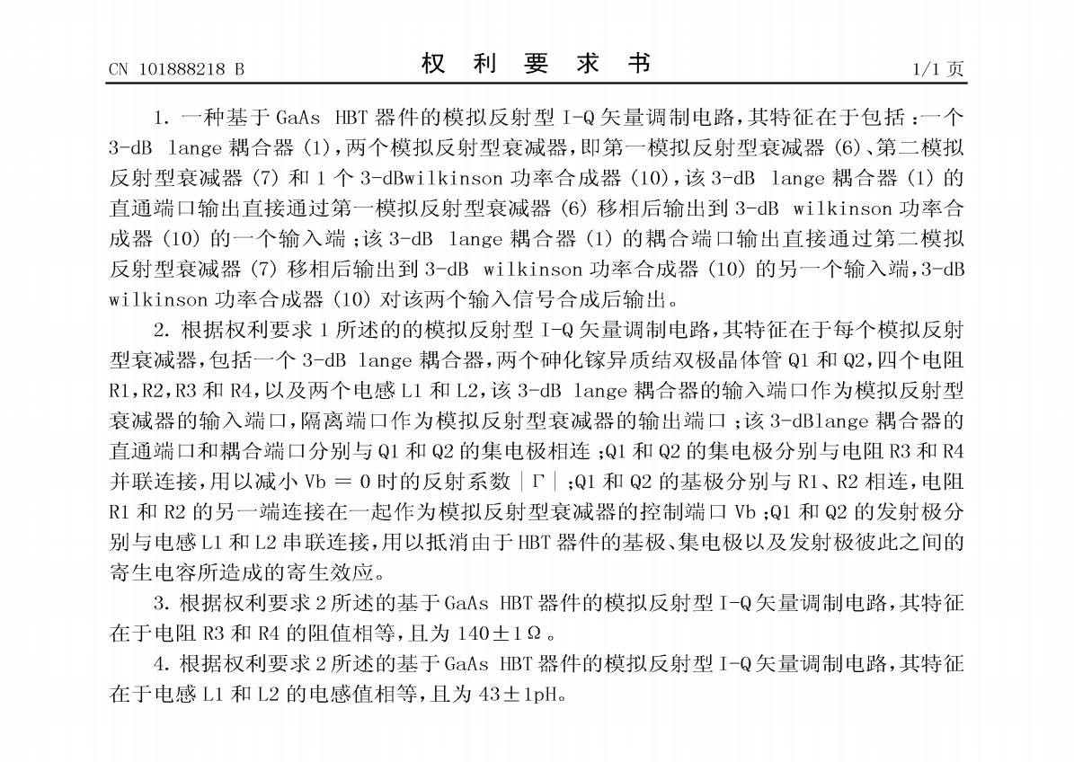
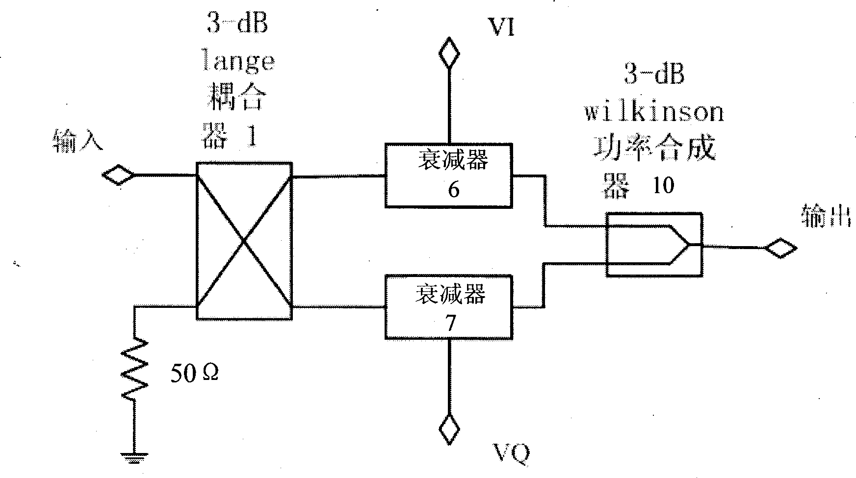
【 中文摘要 】本发明公开了一种基于GaAs HBT器件的模拟反射型I-Q矢量调制电路,主要解决现有调制电路占用芯片面积比大,成本高的问题。其包括:一个3-dB lange耦合器(1),两个模拟反射型衰减器(6,7),和1个3-dB wilkinson功率合成器(10),该3-dB lange耦合器的直通端口输出直接通过第一衰减器(6)移相后输出到功率合成器(7)的一个输入端;该3-dB lange耦合器的耦合端口输出直接通过第二衰减器(6)移相后输出到功率合成器(10)的另一个输入端,其中每个模拟反射型衰减器的砷化镓异质结双极晶体管,其集电极分别并联连接有电阻R3和R4,用以减小Vb=0时的反射系数|Γ|,其发射极分别串联连接有电感L1和L2,用以抵消由于HBT器件的寄生效应。本发明可用于产生I-Q调制信号或者进行频率转换。
【 英文摘要 】The invention discloses a simulated reflection type I-Q vector modulation circuit based on a GaAs (Generally accepted Auditing standards) HBT (Heterojunction Bipolar Transistor) device, mainly solving the problems of large chip-occupied area ratio and high cost of the traditional modulation circuit and comprising a 3-dB Lange coupler (1), two simulated reflection type attenuators (6, 7) and a 3-dB Wilkinson power combiner (10), wherein the straight-through port of the 3-dB Lange coupler is outputted to one input end of the power combiner (10) after directly subjected to phase shift by the first attenuator (6), and the coupling port of the 3-dB Lange coupler is outputted to the other input end of the power combiner (10) after directly subjected to phase shift by the second attenuator (7), wherein the collector electrodes of a gallium arsenide hetero-junction bipolar transistor of each simulated reflection type attenuator are respectively connected with resistors R3 and R4 in parallel for reducing a reflection factor gamma when Vb is equal to 0, and the transmission electrodes of the gallium arsenide hetero-junction bipolar transistors are respectively connected with inductors L1 and L2 in series for offsetting a parasitic effect generated by the HNT device. The invention can be used for generating I-Q modulation signals or carrying out frequency conversion.


